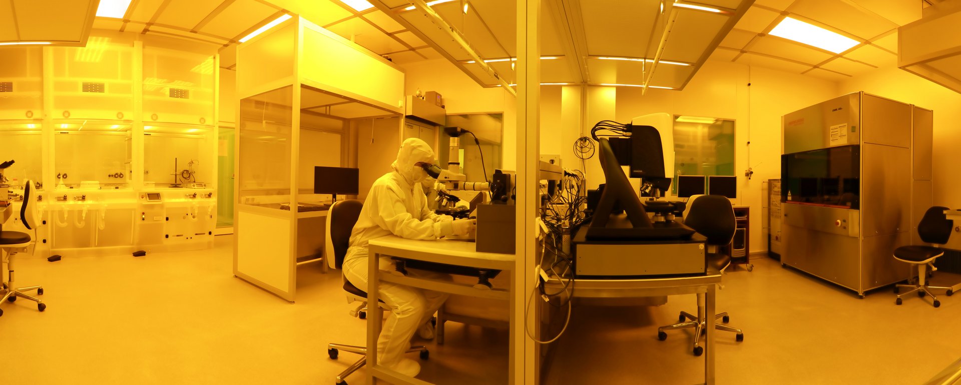
The chair for microsystems technology has facilities for the preparation of semiconductor micro- and nanostructures.
These include, among others:
| Plasma incinerator |
| Spin coater |
| Laser lithography system (structure widths > 600 nm) |
| Scanning electron miscroscope / electron beam lithography system |
| Inert gas glove box with spin coater and Ozone Cleaner |
| Plasma etching machine (ICP-RIE) |
| Evaporation systems |
| Wafer saws |
| Plasma coating system (ICPECVD) |
| Tempering systems |
| Scoring device |
During the preparation, the components and systems are characterized with the following devices:
- optical miscroscopes
- Ellipsometer
- Interference microscope
- Confocal microscope
- Scanning probe microscopes (AFM, MFM)
Several cryostats (temperature range: 300 mK to 500 K) and electromagnets and superconducting magnets (up to 17 T) are available for magnetic field-dependent and temperature-dependent measurements. The electrical characterization is carried out using semiconductor parameter analyzers, lock-in technology (up to f = 200 MHz) and capacitance-voltage measuring devices.
")
")
")
")

")
")
")
")
")
")
")
")
")
")
")
")
")
")
")